
电子/通讯类
To design a CMOS invertor with balance rise and fall time,please define the ration of channel width of PMOS and NMOS and explain?
题目
To design a CMOS invertor with balance rise and fall time,please define the ration of channel width of PMOS and NMOS and explain?
相似问题和答案
第1题:
此题为判断题(对,错)。
第2题:
please show the CMOS inverter schmatic,layout and its cross sectionwith P-well process.Plot its transfer curve (Vout-Vin) And also explain the operation region of PMOS and NMOS for each segment of the transfer curve? (威盛笔试题c ircuit design-beijing-03.11.09)
第3题:
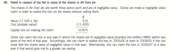
(ii) Explain, with reasons, the relief available in respect of the fall in value of the shares in All Over plc,
identify the years in which it can be claimed and state the time limit for submitting the claim.
(3 marks)
第4题:
To design a CMOS invertor with balance rise and fall time,please define
the ration of channel width of PMOS and NMOS and explain?
第5题:
什么是NMOS、PMOS、CMOS?什么是增强型、耗尽型?什么是PNP、NPN?他们有什么差别?(仕兰微面试题目)
第6题:
第7题:
please draw the transistor level schematic of a cmos 2 input AND gate and explain which input has faster response for output rising edge.(less delay time)。(威盛笔试题circuit design-beijing-03.11.09)
第8题:
A.brief and to the point
B.to work hard
C.to rise or fall
第9题:
Please explain how we describe the resistance in semiconductor. Compare the resistance of a metal,poly and diffusion in tranditional CMOS process.(威盛笔试题circuit design-beijing-03.11.09)
第10题:
please draw the transistor level schematic of a cmos 2 input AND gate and
explain which input has faster response for output rising edge.(less delay
time)。(威盛笔试题circuit design-beijing-03.11.09)